
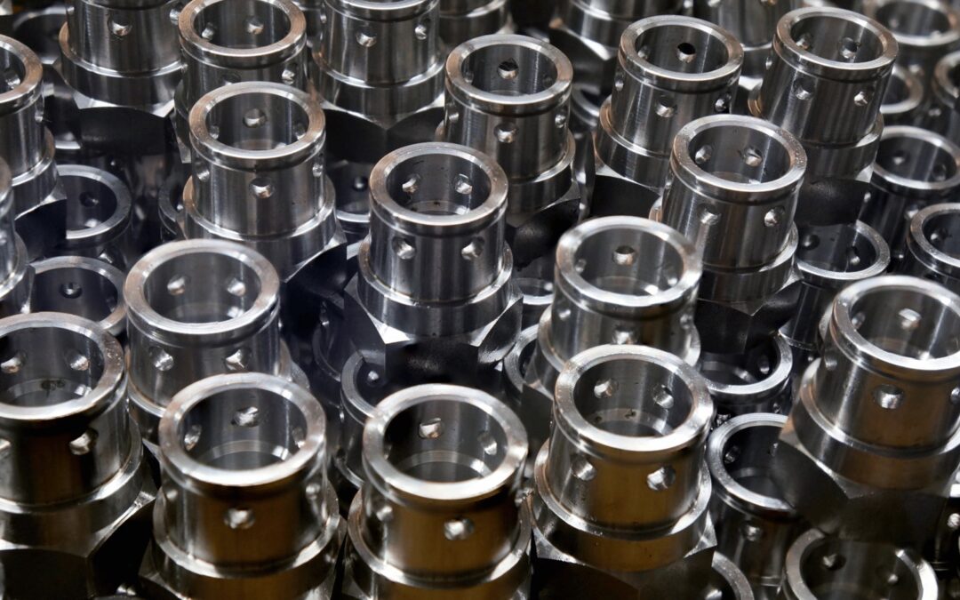
Semiconductor manufacturing operates at atomic scales where micro-level flaws create multi-million-dollar yield losses. As chip architectures shrink toward advanced sub-nanometer nodes, semiconductor equipment must handle extreme processing conditions without introducing defect-causing impurities.
WessDel delivers specialized semiconductor precision machining services designed to meet these exacting demands. We manufacture critical vacuum chamber components, wafer-handling hardware, and lithography tooling built to withstand aggressive fabrication environments.
The Brutal Environments Inside Semiconductor Fabrication Tools
Modern semiconductor fabrication subjects chamber components to continuous operational stress. Deposition, etch, and lithography processes rely on hyper-aggressive conditions that rapidly degrade standard materials:
- Corrosive Plasma Gases: Fluorine- and chlorine-based reactive plasmas erode internal chamber walls, risking contamination.
- Extreme Vacuums: High-vacuum and ultra-high-vacuum (UHV) systems cause microscopic material outgassing if components contain trace impurities or trapped fluids.
- Thermal Cycling: Rapid shifts in process temperatures induce thermal expansion stresses that alter critical dimensions.
To prevent structural failure and maintain tool uptime, high-end fabrication tools require components built with zero chemical or particulate tolerance. Achieving absolute dimensional repeatability across lithography and deposition systems ensures consistent wafer yields batch after batch.
Specialized Material Processing for the Chipmaking Industry
Machining components for wafer processing tools requires deep expertise in difficult-to-machine, high-purity materials. Standard metal-cutting practices do not work when preparing components for cleanroom operations.
At WessDel, our team applies specialized machining strategies tailored to critical semiconductor materials:
- Specialty Polymers: Processing engineered plastics like PEEK, Torlon, and Teflon without inducing thermal stress or surface degradation.
- Clean Machining Protocols: Using clean-cutting fluids and dedicated tooling setups to stop cross-contamination before it starts.
- Ultra-Smooth Surface Finishing: Achieving precise surface roughness parameters (Ra) to eliminate surface microscopic pockets where particles accumulate.
Proper surface execution directly extends component lifespan and prevents particle generation inside plasma chambers.
Strict Inspection and Ultra-Clean Packaging Standards
A precision-machined part is only as good as its cleanliness upon delivery. Raw machining accuracy means little if microscopic contaminants reach a cleanroom floor.
We maintain rigorous quality assurance protocols at every stage of production:
- Non-Contact Metrology: We verify geometric tolerances using advanced non-contact measuring equipment to prevent surface scratches on delicate quartz or ceramic parts.
- Multi-Stage Ultrasonic Cleaning: Components undergo automated multi-bath ultrasonic wash cycles to strip away all residual cutting fluids, particulates, and surface oils.
- Cleanroom Packaging: Cleaned parts pass directly into controlled environments for vacuum sealing in ultra-pure double bags, protecting them during transit to your wafer fabrication location.
Supporting Next-Gen Microelectronics Nodes with WessDel
Next-generation microelectronics require suppliers who understand the rigorous physics of semiconductor tools. WessDel brings more than 50 years of high-precision manufacturing experience to complex wafer processing challenges. Whether you need custom prototypes or scaled production runs, our team delivers high-yield reliability for your critical assemblies.
Contact WessDel for Semiconductor Precision Machining Services Today
Partner with a team that understands micro-precision execution and contamination control. Contact WessDel today to discuss your application and learn how our precision machining for semiconductor equipment keeps your tools performing at peak efficiency.